EX-403 · Digital Electronics Logic Design/Unsolved PYQ Paper
EX-403 Digital Electronics and Logic Design (DELD) - Jun 2023 Question Paper
Under each question, How to answer lists the points an answer should cover, outlined by CampusPrep from the syllabus. Check the details against your textbook.
-
7 MarksaConvert the following codes.
- i)$(785.B2)_{16} = (\quad)_{10}$
- ii)$(1011011.1101)_{2} = (\quad)_{8}$
- iii)$(110101.101101)_{2} = (\quad)_{Gray}$
- iv)$(751.231)_{8} = (\quad)_{16}$
How to answer
- State each conversion method base to base
- Show calculation for (785.B2)16 to decimal
- Group bits for binary-octal and octal-hex conversions
- Binary to Gray conversion rule
-
7 MarksbUse the tabulation procedure to generate the set of prime implicates and to obtain all minimal expression for $$F_{1} = (w,x,y,z) = \sum(1,5,6,12,13,14) + \sum \phi(10,4)$$
How to answer
- List minterms and don't cares
- Apply Quine-McCluskey tabulation steps
- Identify prime implicates
- Select all minimal SOP expressions
-
7 MarksaFind the minimal SOP expression for the function $f(x,y,z) = \Sigma m (0, 2, 3, 5, 6, 7)$
How to answer
- Plot 3-variable K-map for minterms 0,2,3,5,6,7
- Form largest groups of 1s
- Write product term for each group
- Give minimal SOP sum
-
7 MarksbWhat do you understand by Subtractor? Explain the working principle of half subtractor using suitable diagram and truth table.
How to answer
- Define subtractor and need for subtraction
- Truth table of half-subtractor (Difference, Borrow)
- Logic expressions $D = A \oplus B$, $B_o = \bar{A}B$
- Circuit diagram using gates and working
-
7 MarksaRealize the Boolean expression $Z = ABC + AD + CD'$ using NAND gates only.
How to answer
- Write given expression $Z = ABC + AD + CD'$
- Apply double inversion for NAND-NAND form
- Show realization using NAND gates only
- Neat logic diagram
-
7 MarksbDefine decoder. Construct $3 \times 8$ decoder using logic gates.
How to answer
- Define decoder
- Truth table of 3-to-8 decoder
- Logic expressions for 8 outputs using AND/NOT
- Circuit diagram with 3 inputs and 8 outputs
-
7 MarksaDraw a neat circuit diagram of a negative edge triggered JK flip-flop and explain its operation.
How to answer
- Circuit diagram of negative edge triggered JK flip-flop
- Function of J,K, clock and master-slave or edge detector
- Truth/characteristic table operation
- Waveform or working for set, reset, hold, toggle
-
7 MarksbPrepare the state table and excitation table for the Sequential machine shown below. Use T flip flop.
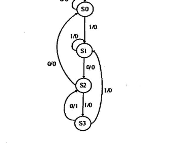
How to answer
- Read state diagram with states S0-S3 and input/output labels
- Assign binary codes and derive next-state table
- Use T flip-flop excitation $T = Q \oplus Q^+$ to get excitation table
- Present state table and excitation table
-
7 MarksaDraw a neat circuit diagram of positive edge triggered D flip-flop and explain its operation.
How to answer
- Circuit diagram of positive edge triggered D flip-flop
- Role of D, clock and edge detector/latches
- Truth table Q+ = D operation
- Waveform explanation
-
7 MarksbDraw and explain the working of Johnson Counter.
How to answer
- Circuit diagram of Johnson counter with inverted feedback
- Sequence of states for n flip-flops
- Modulus 2n operation and timing
- Advantages/applications
-
7 MarksaDraw a 4-bit Asynchronous UP counter and discuss its characteristics. Draw the waveforms.
How to answer
- Circuit of 4-bit ripple UP counter using JK/T flip-flops
- Clocking connection Q to next clock
- Timing waveforms Q0-Q3 0000 to 1111
- Characteristics: propagation delay, modulus 16
-
7 MarksbWhat are the different types of registers? Explain the Parallel Input Serial Output shift register.
How to answer
- List types: SISO, SIPO, PISO, PIPO, bidirectional
- Circuit of PISO shift register
- Loading parallel data then shifting out serially
- Timing operation
-
7 MarksaWhat are sequential programmable devices? Draw the sequential programmable logic for a basic microcell logic.
How to answer
- Define sequential programmable devices (SPLD/CPLD/FPGA context)
- Basic microcell components: AND-OR, flip-flop, feedback
- Diagram of microcell logic
- Programmability aspect
-
7 MarksbExplain the working of successive approximation ADC. Mention the advantages and disadvantages.
How to answer
- Block diagram of SAR ADC: comparator, DAC, SAR
- Step-by-step binary search conversion process
- Advantages: speed, resolution
- Disadvantages: complexity, cost
-
14 MarksWrite a short notes on any Two:
- i)BCD Adder
- ii)Parity Generator
- iii)Priority Encoder
- iv)Decoding in Counter
How to answer
- Select any two topics from list
- Principle/circuit diagram for each
- Working with truth table/logic
- Applications
Go to where you left off?
Quick Add to Notes
Save questions, your own notes and screenshots into notes filed by unit. It takes a free account.
Create free accountHave an account? Log in
Notes Panel