IT-305 · Digital Circuits and Systems/Unsolved PYQ Paper
IT-305 Digital Circuits and Systems - Dec 2023 Question Paper
Under each question, How to answer lists the points an answer should cover, outlined by CampusPrep from the syllabus. Check the details against your textbook.
-
7 MarksaConvert the following numbers to their equivalent in indicated bases: i) $(5321)_6 = (\quad)_{11}$ ii) $(178)_9 = (\quad)_6$ iii) $(123)_8 = (\quad)_{10}$
How to answer
- Convert $(5321)_6$ to base 10: $5\times 6^3 + 3\times 6^2 + 2\times 6^1 + 1\times 6^0 = 1080 + 108 + 12 + 1 = 1201_{10}$; convert to base 11 by successive division.
- Convert $(178)_9$ to base 10: $1\times 9^2 + 7\times 9^1 + 8\times 9^0 = 81 + 63 + 8 = 152_{10}$; convert to base 6 by successive division.
- Convert $(123)_8$ to base 10: $1\times 8^2 + 2\times 8^1 + 3\times 8^0 = 64 + 16 + 3 = 83_{10}$.
-
7 MarksbDesign a 4-bit BCD to Excess-3 code convertor and realize it using 2-level gate implementation.
How to answer
- Construct truth table with BCD inputs (0000 to 1001) and Excess-3 outputs (0011 to 1100), with 1010 to 1111 as don't-cares.
- Draw Karnaugh maps for each output bit: $W$, $X$, $Y$, $Z$.
- Derive minimal SOP expressions for all four output variables.
- Draw the 2-level AND-OR logic circuit schematic.
-
7 MarksaDesign a digital circuit which converts a 3-bit binary number into its equivalent 1's compliment form.
How to answer
- State definition of 1's complement: inverting each bit.
- Provide truth table for 3-bit binary input ($A, B, C$) and outputs ($A', B', C'$).
- Show simplified Boolean expressions: each bit is simply complemented ($Y_2 = \overline{A}$, $Y_1 = \overline{B}$, $Y_0 = \overline{C}$).
- Draw circuit diagram using three NOT gates or XOR gates with control line tied high.
-
7 MarksbDraw the logic diagram of an 8-to-3 line encoder. Explain its operation using truth table.
How to answer
- Define 8-to-3 line encoder function (8 input lines $D_0-D_7$, 3 output binary lines $Y_2, Y_1, Y_0$).
- Draw complete truth table indicating active-high input lines and corresponding 3-bit output codes.
- Derive Boolean equations for outputs: $Y_2 = D_4 + D_5 + D_6 + D_7$, $Y_1 = D_2 + D_3 + D_6 + D_7$, $Y_0 = D_1 + D_3 + D_5 + D_7$.
- Draw logic diagram using three 4-input OR gates.
-
7 MarksaExplain the operation of a priority encoder. Design and draw the logic diagram of the same.
How to answer
- Explain the working principle of a priority encoder resolving simultaneous active inputs based on priority.
- Present the truth table for a 4-input priority encoder ($D_3, D_2, D_1, D_0$) including don't care conditions ('X') and valid output bit $V$.
- Derive simplified Boolean expressions for outputs ($X, Y, V$) using K-maps.
- Draw the logic circuit diagram using basic gates.
-
7 MarksbImplement the following Boolean functions using $4 \times 1$ multiplexer and external logic gates. Connect inputs 'A' and 'C' to select lines. $$F(A, B, C, D) = \Sigma(0, 3, 5, 6, 8, 9, 11, 13, 15)$$
How to answer
- Identify select lines $S_1 = A, S_0 = C$ and remaining variables as $B$ and $D$.
- Construct an implementation table (or minterm partition table) for the 4 combinations of $AC$: $00, 01, 10, 11$.
- Determine the data input functions $I_0, I_1, I_2, I_3$ in terms of $B$ and $D$ for each combination.
- Implement necessary functions of $B, D$ using external logic gates and connect them to inputs $I_0, I_1, I_2, I_3$ of the $4 \times 1$ MUX.
- Draw the complete circuit schematic showing the $4 \times 1$ MUX and external gates.
-
7 MarksaImplement a full adder using a decoder and NAND gates only. The inputs to the adder are 'A', 'B' and 'C' and the outputs are 'S' and '$\text{C}_{\text{out}}$'.
How to answer
- Express Full Adder outputs in minterm form: $S = \Sigma m(1, 2, 4, 7)$ and $C_{\text{out}} = \Sigma m(3, 5, 6, 7)$.
- Explain that an active-low 3-to-8 decoder outputs $\overline{m_i}$, and a NAND gate acts as an OR of minterms: $\overline{\overline{m_a} \cdot \overline{m_b} \cdots} = m_a + m_b + \cdots$.
- Connect decoder inputs to $A, B, C$.
- Connect decoder outputs $1, 2, 4, 7$ to a NAND gate for $S$, and outputs $3, 5, 6, 7$ to another NAND gate for $C_{\text{out}}$.
- Draw the circuit diagram.
-
7 MarksbDesign a full subtractor using only required number of half subtractors.
How to answer
- Define equations for half subtractor: $D = A \oplus B$, $B_{\text{out}} = \overline{A} B$.
- Define equations for full subtractor: $D = A \oplus B \oplus C$, $B_{\text{out}} = \overline{A}B + \overline{(A \oplus B)}C$.
- Show implementation using two half subtractors and an OR gate.
- Provide logic/block diagram showing connections between the two half subtractors and the OR gate.
-
7 MarksaConvert a D flip-flop into J-K flip-flop. Show all the necessary calculations with final logic diagram. Use only 2-input NAND gates to realise any Boolean function required for this conversion.
How to answer
- Set up conversion table with inputs $J, K$, present state $Q_n$, next state $Q_{n+1}$, and required D flip-flop input $D$.
- Simplify $D$ using K-map: $D = J\overline{Q}_n + \overline{K}Q_n$.
- Express $D$ in NAND-only form: $D = \overline{\overline{J\overline{Q}_n} \cdot \overline{\overline{K}Q_n}}$, converted to 2-input NAND gates.
- Draw circuit diagram showing 2-input NAND gates driving the D input of D flip-flop.
-
7 MarksbDesign an asynchronous MOD-4 DOWN counter using T flip-flop.
How to answer
- State number of flip-flops required: $n = 2$ ($2^2 = 4$).
- List counting sequence: $3 (11) \to 2 (10) \to 1 (01) \to 0 (00) \to 3 (11)$.
- Explain clock triggering logic: for negative-edge-triggered flip-flops, connect $Q$ output of first flip-flop to clock input of the next, or for positive-edge, connect $\overline{Q}$.
- Set $T_0 = T_1 = 1$ (Vcc) for toggle mode.
- Draw schematic diagram and timing diagram of the MOD-4 down counter.
-
7 Marksa
Draw the logic diagram of a universal shift register. Assume $(S_1, S_0)$ are the mode control pins, such that the register observes following modes of operation:
Mode Control $S_1$ Mode Control $S_0$ Register operation 0 0 No change 0 1 Shift right 1 0 Shift left 1 1 Parallel load How to answer
- Explain architecture of a 4-bit universal shift register using four 4x1 MUXes and four D flip-flops.
- List functions of select lines $S_1, S_0$ for inputs $I_0$ (Hold/No change), $I_1$ (Shift Right), $I_2$ (Shift Left), and $I_3$ (Parallel Load).
- Draw complete schematic diagram showing connections between 4x1 MUXes, D flip-flops, serial inputs, and parallel data lines.
-
7 MarksbExplain the operation of a 2-input TTL NOR gate.
How to answer
- Draw the internal circuit schematic of a 2-input TTL NOR gate with totem-pole output.
- Explain circuit operation for inputs: Low-Low, Low-High, High-Low, and High-High.
- Show state of transistors (saturation/cutoff) for each input case.
- Provide truth table confirming NOR logic operation.
-
7 MarksaDesign a 2-input NOR gate using PMOS logic and explain its operation.
How to answer
- Explain PMOS conduction behavior (conducts when gate is low relative to source).
- Draw circuit diagram of 2-input PMOS NOR gate (parallel driver PMOS transistors with a load PMOS / resistor).
- Detail operation for all 4 input binary combinations ($00, 01, 10, 11$).
- Verify output corresponds to NOR function.
-
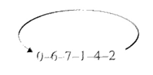
7 MarksbDesign a synchronous counter to count the following sequence using JK flip flop: $$0-6-7-1-4-2$$
How to answer
- Determine number of flip-flops: max count is 7, so 3 flip-flops ($A, B, C$) are needed.
- List state transition sequence: $000 \to 110 \to 111 \to 001 \to 100 \to 010 \to 000$; states 3 ($011$) and 5 ($101$) are unused (don't cares).
- Create excitation table using JK flip-flop excitation values for each transition.
- Minimize input equations ($J_A, K_A, J_B, K_B, J_C, K_C$) using Karnaugh maps.
- Draw synchronous logic circuit diagram connecting all JK flip-flops to a common clock.
-
7 MarksaExplain the operation of an LCD display. What is the typical difference between an LED display and an LCD display?
How to answer
- Explain operating principle of LCD (polarizers, liquid crystal molecules alignment modulated by electric field, light modulation).
- Mention construction (glass plates, transparent electrodes, liquid crystal layer).
- Provide comparison between LED and LCD: active light emitter vs passive light modulator, power consumption (LED high, LCD very low), response time, visibility in bright sunlight.
-
7 MarksbExplain the operation of a Successive-Approximation type of Analog-to-digital convertor.
How to answer
- Draw block diagram of Successive Approximation ADC showing comparator, SAR, DAC, and control logic.
- Explain step-by-step conversion process based on binary search algorithm starting from MSB to LSB.
- Explain role of comparator in keeping or clearing the trial bit.
- State conversion time characteristics: $n$ clock cycles for $n$-bit resolution.
- Mention advantages (fast conversion speed, fixed conversion time).
Go to where you left off?
Quick Add to Notes
Save questions, your own notes and screenshots into notes filed by unit. It takes a free account.
Create free accountHave an account? Log in
Notes Panel