EC-304 · Electronic Devices/Unsolved PYQ Paper
EC-304 Electronic Devices - Dec 2025 Question Paper
Under each question, How to answer lists the points an answer should cover, outlined by CampusPrep from the syllabus. Check the details against your textbook.
-
7 MarksaState the law of junction relating the boundary value of injected minority carrier concentration with applied voltage? How does the avalanche breakdown voltage vary with temperature?
How to answer
- State law of junction for injected minority carrier boundary concentration: p_n(0)=p_n0 exp(V/V_T) etc.
- Explain dependence on applied voltage and thermal voltage
- Define avalanche breakdown mechanism
- Explain positive temperature coefficient - breakdown voltage increases with temperature due to reduced mean free path
-
7 MarksbBriefly discuss about the following:
- i)LED & solar cell
- ii)Zener diode as a voltage regulator
How to answer
- LED principle: radiative recombination, materials, applications
- Solar cell principle: photovoltaic effect, construction
- Zener diode reverse breakdown for regulation
- Regulator circuit operation with series resistor and load
-
7 MarksaExplain the working of bridge rectifier. Give the Expression for RMS current, PIV, Ripple factor and efficiency.
How to answer
- Bridge rectifier circuit with 4 diodes and operation in both half cycles
- Waveforms and current paths
- Derive expressions for RMS current, PIV, ripple factor
- Derive efficiency formula ~81.2%
-
7 MarksbDetermine and draw the output voltage of given network.
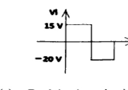
How to answer
- Identify clamper circuit with Si diode, 5V battery, R-RL and capacitor C
- Use input square wave +15V to -20V to find capacitor voltage
- Determine clipping/clamping levels for both half cycles
- Sketch output voltage waveform with DC shift
-
7 MarksaExplain the selection of Q point for a transistor bias circuit and discuss the limitations on the output voltage swing.
How to answer
- Need for Q-point and DC load line concept
- Criteria for selection in active region for undistorted output
- Effect of Q-point near saturation/cutoff on clipping
- Limitations on output voltage swing: Vce(max), Ic(sat), power dissipation
-
7 MarksbDesign a voltage divider bias circuit for transistor to establish the quiescent point at $V_{CE}=12V$, $I_C=1.5mA$, stability factor $S\le3$, $\beta=50$, $V_{BE}=0.7V$, $V_{CC}=22.5V$ and $R_C=5.6k\Omega$.
How to answer
- Given V_CE=12V, I_C=1.5mA, S<=3, beta=50, V_BE=0.7V, V_CC=22.5V, R_C=5.6kohm
- Apply stability factor condition to find R_E and divider currents
- Calculate R1, R2 using Thevenin equivalent
- Verify Q-point and stability
-
7 MarksaState the reason for fall in gain at low and high frequencies. Why is the Miller effect reduced in a cascade amplifier?
How to answer
- Coupling/bypass capacitors cause fall at low frequencies
- Interelectrode and stray capacitances cause fall at high frequencies
- Miller multiplication of feedback capacitance
- Why cascode reduces Miller effect due to low input resistance of CB stage
-
7 MarksbAnalyze the V-I characteristics, output resistance, minimum sustainable voltage, and maximum usable load of a current mirror.
How to answer
- Current mirror principle and V-I characteristics
- Output resistance due to Early effect
- Minimum sustainable (compliance) voltage
- Maximum usable load determination
-
7 MarksaExplain working principle of Depletion type MOSFET (n-channel). Draw & Explain its characteristics.
How to answer
- Depletion MOSFET n-channel structure and operation
- Working with zero, positive and negative Vgs
- Drain and transfer characteristics curves
- Diagram of device cross-section and symbols
-
7 MarksbDescribe about small signal MOSFET amplifiers (NMOS) and obtain the expression for its trans conductance.
How to answer
- Small-signal NMOS amplifier configuration
- Small-signal model and transconductance definition gm
- Derivation of gm = 2ID/Vov = sqrt(2 mu Cox W/L ID)
- Frequency and bias dependence
-
7 MarksaWhy is common collector mode generally not preferred? Increase in collector emitter voltage from 5V to 8V causes increase in collector current from 5mA to 5.3mA. Determine the dynamic output resistance.
How to answer
- Common collector voltage gain <1, use as buffer
- Dynamic output resistance r_o = delta V_CE / delta I_C
- Calculate (8-5)V/(5.3-5.0)mA = 10kohm
- Reason for not preferred for voltage amplification
-
7 MarksbDescribe the construction and working of UJT with its equivalent circuit and V-I characteristics.
How to answer
- UJT structure: n-type bar with p-emitter, B1 B2 bases
- Equivalent circuit with R_B1, R_B2 and diode
- Working: cutoff, negative resistance, saturation regions
- V-I characteristics with Vp, Vv, Ip, Iv points
-
7 MarksaWhat is harmonic distortion? How does it arise in Class B-operation? And, how can it be corrected in push-pull circuit?
How to answer
- Definition of harmonic distortion and THD
- Class-B crossover and nonlinearity causing harmonics
- Push-pull cancellation of even harmonics
- Matching and biasing to minimize residual distortion
-
7 MarksbDetermine the thermal equilibrium electron and hole concentrations for a given doping concentration. Consider a germanium sample at T = $300^oK$ in which $N_d = 5 \times 10^{13} cm^{-3}$ and Na = 0. Assume that $n_i = 2.4 \times 10^{13} cm^{-3}$.
How to answer
- Charge neutrality n0 + Na = p0 + Nd and mass action n0 p0 = ni^2
- Solve quadratic for n0 with Nd=5x10^13, Na=0, ni=2.4x10^13
- Calculate n0 ~5.9x10^13 cm-3 approx and p0 = ni^2/n0
- Interpretation as n-type germanium
-
14 MarksWrite short notes on any **two** the following:
- a)Voltage regulation using IC
- b)Ebers-Moll model
- c)Darlington amplifier
How to answer
- Voltage regulation using IC: series/shunt regulator IC principle
- Ebers-Moll model: coupled diode equations for BJT
- Darlington amplifier: compound pair, high beta, applications
- Any two with circuit diagram and key expressions
Go to where you left off?
Quick Add to Notes
Save questions, your own notes and screenshots into notes filed by unit. It takes a free account.
Create free accountHave an account? Log in
Notes Panel