EC-304 · Electronic Devices/Unsolved PYQ Paper
EC-304 Electronic Devices - Dec 2023 Question Paper
Under each question, How to answer lists the points an answer should cover, outlined by CampusPrep from the syllabus. Check the details against your textbook.
-
7 MarksaDefine elemental and compound semiconductor materials with examples and draw energy band diagram for intrinsic and extrinsic silicon.
How to answer
- Definition of elemental semiconductors (single-element like Si, Ge) with examples.
- Definition of compound semiconductors (composed of two or more elements like GaAs, InP) with examples.
- Energy band diagram of intrinsic silicon showing valence band, conduction band, and Fermi level $E_F$ in the middle of the band gap.
- Energy band diagram of extrinsic silicon (n-type and p-type) showing the shift in Fermi level relative to conduction and valence bands.
-
7 MarksbDraw V-I characteristics and write applications of following special purpose diodes: i) Tunnel diode ii) Photo diode iii) Schottky diode
How to answer
- Tunnel diode: V-I curve showing peak current, valley current, and negative resistance region; list applications (microwave oscillators, high-speed switching).
- Photodiode: Reverse-bias V-I curve parameterized by illumination levels; list applications (optical detectors, light meters, optical fiber communication).
- Schottky diode: V-I curve showing low forward voltage drop and fast switching; list applications (clamping, RF mixers, power rectifiers, switch-mode power supplies).
-
7 MarksaExplain the working of simple clipper and clamper with circuit diagram.
How to answer
- Clipper circuit: Circuit diagram of series/shunt diode clipper, operation during positive and negative half cycles, input/output waveforms.
- Clamper circuit: Circuit diagram of positive or negative clamper (diode, capacitor, resistor), charging and discharging of capacitor, DC level shifting, input/output waveforms.
-
7 MarksbDescribe the working of half wave and full wave bridge rectifier circuits with circuit diagram.
How to answer
- Half-wave rectifier: Schematic diagram, operation during positive and negative cycles, output voltage waveform.
- Full-wave bridge rectifier: Circuit diagram with four diodes ($D_1-D_4$), operation during alternate half cycles, output waveform.
- Brief comparison of performance parameters (efficiency, PIV, ripple factor).
-
7 MarksaWrite name of mode of operation and configurations for BJT. Also describe basic construction and operation.
How to answer
- Modes of operation: Cutoff, Active, Saturation, and Inverted/Reverse active based on junction biases.
- Configurations: Common Emitter (CE), Common Base (CB), Common Collector (CC).
- Basic construction: NPN and PNP structures, doping levels and widths of Emitter, Base, and Collector.
- Operation: Injection of charge carriers from emitter, recombination in base, and collection by collector.
-
7 MarksbWhat is need of biasing? Write name of different biasing techniques used in BJT and describe any one in detail.
How to answer
- Need of biasing: Establishing a stable Q-point in the active region to avoid distortion and thermal runaway.
- List of biasing circuits: Fixed bias, Collector-to-base bias, Voltage divider bias, Emitter bias.
- Detailed explanation of one method (e.g., Voltage Divider Bias): Circuit diagram, derivation of $I_C$ and $V_{CE}$, stability factor analysis.
-
7 MarksaDiscuss following in brief: i) Darlington amplifier and Cascode amplifier ii) Low and high frequency response iii) Coupling methods in multistage amplifier
How to answer
- Darlington & Cascode amplifiers: Configurations, key features (high current gain / high input impedance for Darlington; high bandwidth / reduced Miller effect for Cascode).
- Frequency response: Gain variation at low frequencies (due to coupling and bypass capacitors) and high frequencies (due to parasitic capacitances and carrier transit time).
- Coupling methods: RC coupling, Transformer coupling, Direct coupling, along with their pros and cons.
-
7 MarksbPerform analysis of common emitter amplifier using h-parameter.
How to answer
- Draw CE small-signal AC equivalent model using h-parameters ($h_{ie}, h_{re}, h_{fe}, h_{oe}$).
- Derive expression for Current Gain: $A_i = -\frac{h_{fe}}{1 + h_{oe} R_L}$.
- Derive expression for Input Impedance: $Z_i = h_{ie} + h_{re} A_i R_L$.
- Derive expression for Voltage Gain: $A_v = \frac{A_i R_L}{Z_i}$.
- Derive Output Admittance: $Y_o = h_{oe} - \frac{h_{fe} h_{re}}{h_{ie} + R_s}$.
-
7 MarksaDescribe following with neat diagram i) Transfer and drain characteristics of JFET and MOSFET ii) UJT and Thyristors iii) Common Source (CS) and Common Gate (CG) configurations
How to answer
- Transfer and drain curves for JFET and depletion/enhancement MOSFETs with key parameters labeled ($I_{DSS}, V_P, V_{th}$).
- Basic structure and operational characteristics of UJT (intrinsic standoff ratio $\eta$) and Thyristor/SCR (four-layer device, gate triggering).
- Common Source and Common Gate circuit configurations and their operational features.
-
7 MarksbDerive expression of voltage gain of CS amplifier using hybrid-$\pi$ model.
How to answer
- Draw the small-signal hybrid-$\pi$ equivalent circuit of the Common Source (CS) amplifier.
- Express output voltage $v_o = -g_m v_{gs} (r_d \parallel R_D)$.
- Relate gate-to-source voltage $v_{gs}$ to input voltage $v_i$ ($v_{gs} = v_i$).
- Derive the voltage gain expression: $A_v = \frac{v_o}{v_i} = -g_m (r_d \parallel R_D)$ (or including load $R_L$ and frequency dependence if high-frequency model is assumed).
-
7 MarksaExplain following in brief i) Breakdown mechanism ii) Photo transistor iii) Power amplifiers
How to answer
- Breakdown mechanisms: Zener breakdown (quantum tunneling at high electric field in heavily doped diodes) vs. Avalanche breakdown (impact ionization in lightly doped junctions).
- Phototransistor: Working principle, light-sensitive base region, internal current gain mechanism ($I_C = \beta I_\lambda$).
- Power amplifiers: Definition, classification based on conduction angle (Class A, B, AB, C), efficiency considerations.
-
7 MarksbDetermine the dc bias voltage $V_{CE}$ and the current $I_C$ for the voltage-divider configuration shown in figure (i).
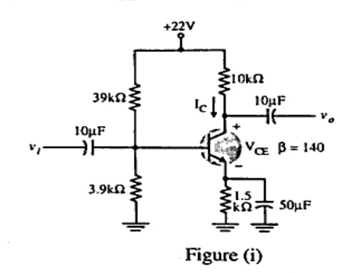
How to answer
- Calculate Thevenin voltage: $V_{TH} = 22 \times \frac{3.9}{39 + 3.9} = 2.0\text{ V}$.
- Calculate Thevenin resistance: $R_{TH} = 39\text{ k}\Omega \parallel 3.9\text{ k}\Omega = 3.55\text{ k}\Omega$.
- Assuming silicon BJT ($V_{BE} = 0.7\text{ V}$), find base current: $I_B = \frac{2.0 - 0.7}{3.55 + 141 \times 1.5}\text{ mA} \approx 0.00604\text{ mA} = 6.04\,\mu\text{A}$.
- Calculate collector current: $I_C = \beta I_B = 140 \times 6.04\,\mu\text{A} \approx 0.846\text{ mA}$.
- Calculate $V_{CE} = V_{CC} - I_C (R_C + R_E) = 22 - 0.846\text{ mA} \times 11.5\text{ k}\Omega \approx 12.27\text{ V}$.
-
7 MarksaDetermine $V_o$ for the network of figure (ii).
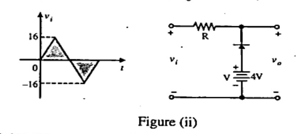
How to answer
- Analyze circuit: Series resistor $R$, parallel branch with downward diode in series with a $+4\text{ V}$ battery (positive terminal facing up).
- For ideal diode: conducts when $v_i > 4\text{ V}$, clipping output voltage to $V_o = 4\text{ V}$.
- When $v_i < 4\text{ V}$: diode is reverse biased (OFF), and $V_o = v_i$.
- Sketch the resulting clipped output waveform ranging between $-16\text{ V}$ and $+4\text{ V}$.
-
7 MarksbWrite note on following i) Ebers-Moll model ii) LED and solar cell iii) Bias stabilization and Thermal runaway
How to answer
- Ebers-Moll model: Large-signal model using two ideal diodes and two dependent current sources; terminal current equations.
- LED and Solar Cell: LED principles (electroluminescence in forward bias); Solar cell principles (photovoltaic effect, generation of electron-hole pairs, I-V quadrant).
- Bias stabilization and Thermal runaway: Temperature dependence of $I_{CO}, V_{BE}, \beta$; cumulative heating leading to device destruction; role of stability factor $S$ and negative feedback.
-
7 MarksaFor the circuit of figure (iii) determine i) $I_{DQ}$ and $V_{GSQ}$ ii) $V_{DS}$
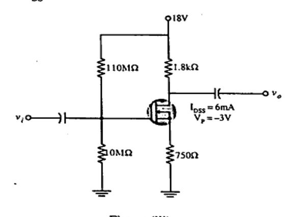
How to answer
- Calculate Gate voltage: $V_G = 18 \times \frac{10\text{ M}\Omega}{110\text{ M}\Omega + 10\text{ M}\Omega} = 1.5\text{ V}$.
- Write gate-to-source loop equation: $V_{GS} = 1.5 - I_D (0.75\text{ k}\Omega)$.
- Substitute into Shockley's equation: $I_D = 6 \left(1 - \frac{V_{GS}}{-3}\right)^2 = 6 \left(1 + \frac{V_{GS}}{3}\right)^2$.
- Solve quadratic equation for $V_{GSQ}$ and obtain $I_{DQ}$ within active region ($V_P < V_{GS} < 0$).
- Calculate $V_{DS} = V_{DD} - I_{DQ} (R_D + R_S) = 18 - I_{DQ} (1.8\text{ k}\Omega + 0.75\text{ k}\Omega)$.
-
7 MarksbWrite notes on following i) UJT relaxation oscillator ii) Transistor as a switch
How to answer
- UJT relaxation oscillator: Circuit schematic, capacitor charging via $R$ to peak point voltage $V_P$, discharge through $R_1$, formula for frequency of oscillation $f = \frac{1}{R C \ln(1/(1-\eta))}$.
- Transistor as a switch: Operation in Cutoff (open switch, $I_C = 0, V_{CE} = V_{CC}$) and Saturation (closed switch, $I_C = I_{C(sat)}, V_{CE} \approx 0.2\text{ V}$); conditions for hard saturation.
Go to where you left off?
Quick Add to Notes
Save questions, your own notes and screenshots into notes filed by unit. It takes a free account.
Create free accountHave an account? Log in
Notes Panel