CS-304 · Digital Systems/Unsolved PYQ Paper
CS-304 CS-304: Digital Systems / CI-304: Digital Circuits and System - Nov 2022 Question Paper
Under each question, How to answer lists the points an answer should cover, outlined by CampusPrep from the syllabus. Check the details against your textbook.
-
7 MarksaGiven the following Boolean function: $F(W, X, Y, Z) = WX'(Y' + Z') + X'.Z'.(W' \odot Y)$ where $\odot$ represents the XNOR operation, determine the simplified(minimal) SOP expression for F using boolean algebra and Implement the given function using NOR-NOR logic.
How to answer
- Expand the XNOR term $(W' \odot Y) = W'Y + WY'$
- Distribute and simplify the expression for $F(W,X,Y,Z)$ using laws of Boolean algebra to find minimal SOP
- Convert the minimal SOP expression into NOR-NOR form using double complementation (De Morgan's laws)
- Draw the circuit diagram using only two-input/multi-input NOR gates
-
7 MarksbCompute the prime implicants (PI) and essential prime implicants (EPI) in the following Boolean function: $$F(W, X, Y, Z) = \Pi M(1, 3, 5, 7, 8, 9, 11, 12) + d(2, 10)$$ Compute a minimal SOP expression for F and determine whether it is unique.
How to answer
- Convert maxterm expression to minterms: $F = \sum m(0, 4, 6, 13, 14, 15) + d(2, 10)$
- Plot minterms and don't cares on a 4-variable K-map (or use Tabulation method)
- Identify all Prime Implicants (PIs)
- Identify Essential Prime Implicants (EPIs) covering unique minterms
- Derive the minimal SOP expression and check if alternative covers exist to determine uniqueness
-
7 MarksaEach of the following functions actually represents a set of four functions, corresponding to the possible assignments of the don't-care terms. $$f_1(w, x, y, z) = \sum(1, 3, 5, 6, 9, 10) + \sum_\phi(11, 12)$$ $$f_2(w, x, y, z) = \sum(0, 3, 4, 5, 8, 9) + \sum_\phi(6, 7)$$ i) Find $f_3 = f_1 \cdot f_2$. How many functions does $f_3$ represent? ii) Find $f_4 = f_1 + f_2$. How many functions does $f_4$ represent?
How to answer
- Analyze truth tables/minterm sets for all 4 combinations of $f_1$ and 4 combinations of $f_2$
- Determine the intersection of $f_1$ and $f_2$ for $f_3 = f_1 \cdot f_2$ across the 16 combinations, identifying certain 1s, certain 0s, and remaining don't-cares
- Compute the number of distinct functions $f_3$ represents
- Determine the union for $f_4 = f_1 + f_2$ similarly and calculate the number of distinct functions represented
-
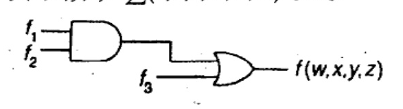
7 MarksbGiven the network of Fig., determine the functions $f_2$ and $f_3$ if $f_1 = xz + x'z'$ and the overall transmission function is to be $$f(w, x, y, z) = \sum(0, 3, 6, 10, 11, 12)$$
How to answer
- Express the circuit equation: $f = f_1 \cdot f_2 + f_3$
- Determine the minterms where $f_1 = 1$ and $f_1 = 0$
- Select $f_2$ and $f_3$ such that their combination covers the required minterms of $f$: {0, 3, 6, 10, 11, 12}
- Simplify expressions for $f_2(w, x, y, z)$ and $f_3(w, x, y, z)$ using K-maps
-
7 MarksaDesign a $8 \times 1$ multiplexer using one $4 \times 1$ multiplexer and four $2 \times 1$ multiplexers.
How to answer
- State the requirement: 8 inputs ($I_0-I_7$), 3 select lines ($S_2, S_1, S_0$), 1 output
- Use four $2 \times 1$ MUXs in the first stage driven by select line $S_0$ to pair inputs $(I_0, I_1), (I_2, I_3), (I_4, I_5), (I_6, I_7)$
- Feed the 4 outputs into the one $4 \times 1$ MUX controlled by select lines $S_2, S_1$
- Draw the complete interconnected block schematic and provide truth table
-
7 MarksbDesign a combinational logic circuit to convert the BCD to excess-3 code.
How to answer
- Construct truth table with 4-bit BCD input ($B_3 B_2 B_1 B_0$) and 4-bit Excess-3 output ($E_3 E_2 E_1 E_0$)
- Define don't care conditions for invalid BCD inputs 10 to 15
- Derive minimized Boolean expressions for $E_3, E_2, E_1, E_0$ using K-maps
- Draw the logic gate implementation diagram
-
7 MarksaDesign a $3 \times 8$ decoder using one $1 \times 2$ decoder and two $2 \times 4$ decoder with Enable input.
How to answer
- Specify inputs $A, B, C$ and outputs $Y_0$ through $Y_7$
- Use the most significant bit $A$ as input to the $1 \times 2$ decoder to generate Enable signals for the two $2 \times 4$ decoders
- Connect inputs $B$ and $C$ in parallel to the select inputs of both $2 \times 4$ decoders
- Draw the circuit/block diagram and give the combined truth table
-
7 MarksbDraw a schematic for a minimal circuit that uses only NOR gates that performs the two's complement operation on a four bit input value. Let the input be $A_{3:0}$ and the output be $B_{3:0}$.
How to answer
- State two's complement logic: $B = A' + 1$
- Write Boolean equations for each output bit $B_0, B_1, B_2, B_3$ in terms of $A_0, A_1, A_2, A_3$ ($B_0 = A_0, B_1 = A_1 \oplus A_0, \dots$)
- Convert each equation into minimal NOR-only logic form
- Draw the complete schematic diagram using only NOR gates
-
7 MarksaCovert Decimal to Binary: i) $(1024)_{10}$ ii) $(23.25)_{10}$
How to answer
- For $(1024)_{10}$: $1024 = 2^{10} = (10000000000)_2$
- For $(23.25)_{10}$: Convert integer part $23 = (10111)_2$
- Convert fractional part $0.25 \times 2 = 0.5$, $0.5 \times 2 = 1.0 \Rightarrow (0.01)_2$
- Combine: $(23.25)_{10} = (10111.01)_2$
-
7 MarksbDraw the state diagram for the following specification sequential systems: Input: $x(t), y(t) \in \{0, 1\}$ Output: $z(t) \in \{0, 1\}$ State: $s(t) \in \{\text{Even}, \text{odd}\}$ Initial state: $s(0) = \text{Even}$ Functions: The transition and output functions are $s(t+1) = \text{even}$ if $x(t)$ and $y(t)$ both are even $s(t+1) = \text{odd}$ otherwise $z(t) = 1$ if $x(t)$ and $y(t)$ both are even $z(t) = 0$ otherwise
How to answer
- Interpret 'even' for binary inputs $x, y \in \{0,1\}$ (typically $0$ is considered even)
- List the 4 input combinations $(x, y) \in \{(0,0), (0,1), (1,0), (1,1)\}$
- Construct the state transition and output table for states {Even, Odd}
- Draw the state diagram showing nodes (Even, Odd), directed transitions with inputs, and outputs
-
7 MarksaDesign a synchronous counter to count in the random sequence $0, 2, 4, 5, 7, 0, 2, 4, 5, 7 \dots$ using D flip-flop.
How to answer
- Determine number of flip-flops required: 3 flip-flops ($Q_2, Q_1, Q_0$) since max count is 7
- Construct state transition table for sequence $0 \to 2 \to 4 \to 5 \to 7 \to 0$, with unused states (1, 3, 6) as don't cares
- Determine D flip-flop inputs ($D = Q_{next}$) for $D_2, D_1, D_0$
- Minimize equations for $D_2, D_1, D_0$ using K-maps
- Draw the logic circuit diagram with D flip-flops and logic gates
-
7 MarksbDesign a sequential circuit using T flip-flop for the following state table. $$\begin{array}{|c|c|c|} \hline \text{Present} & \text{Input } X = 0 & \text{Input } X = 1 \\ \text{State } S(t) & & \\ \hline S_1 & S_1 / 1 & S_4 / 0 \\ S_2 & S_2 / 1 & S_4 / 1 \\ S_3 & S_2 / 1 & S_1 / 0 \\ S_4 & S_4 / 0 & S_2 / 0 \\ \hline \end{array}$$ $$S(t+1) / \text{Output } (Z)$$ Assume any suitable assumptions for state assignment.
How to answer
- Assign binary states to $S_1, S_2, S_3, S_4$ (e.g., $S_1=00, S_2=01, S_3=10, S_4=11$)
- Create transition table and determine excitation values for $T_A$ and $T_B$ using T flip-flop excitation table
- Formulate output $Z$ table from given state outputs
- Simplify expressions for $T_A, T_B$, and $Z$ using K-maps
- Draw the circuit diagram with two T flip-flops and logic gates
-
7 MarksaExplain Interfacing between TTL and MOS with example.
How to answer
- Explain voltage and current compatibility issues ($V_{OH}, V_{OL}, V_{IH}, V_{IL}$ levels)
- Explain TTL driving MOS/CMOS with required pull-up resistor to meet $V_{IH(min)}$
- Explain MOS/CMOS driving TTL and fan-out/current sinking limitations
- Provide schematic diagrams for both TTL-to-MOS and MOS-to-TTL interfacing circuits
-
7 MarksbExplain the concept of working and applications of following memories: i) ROM ii) PLA iii) DRAM iv) FLASH RAM
How to answer
- ROM: Principle of non-volatile storage, diode/transistor array matrix, application in BIOS/firmware
- PLA: Programmable AND and programmable OR arrays, application in implementing complex combinational/sequential logic
- DRAM: Working principle using one transistor and one capacitor cell, need for refresh cycles, application as main computer memory
- FLASH RAM: Floating-gate transistor principle, block-level erasure, application in USB drives, SSDs, smartphones
-
14 MarksWrite notes on the following: i) A/D and D/A convertors ii) CMOS Logic iii) Shannon's theorem for channel capacity iv) Nyquist sampling theorem
How to answer
- A/D and D/A Converters: Principle, resolution, conversion techniques (Flash, Successive Approx, R-2R ladder)
- CMOS Logic: Complementary NMOS/PMOS pull-up and pull-down networks, low power consumption, basic CMOS inverter
- Shannon's Capacity Theorem: $C = B \log_2(1 + \text{SNR})$ in bits/sec, significance of bandwidth and noise limit
- Nyquist Sampling Theorem: Sampling frequency $f_s \ge 2f_m$ to prevent aliasing, reconstruction using low-pass filter
Go to where you left off?
Quick Add to Notes
Save questions, your own notes and screenshots into notes filed by unit. It takes a free account.
Create free accountHave an account? Log in
Notes Panel